

Technology Node

Technology Type
Flash, Logic, BCD, 3D CMOS MEMS, Analog, HV, 3D CIS, NVM, RFOS, Mixed-signal
Factories coorperated
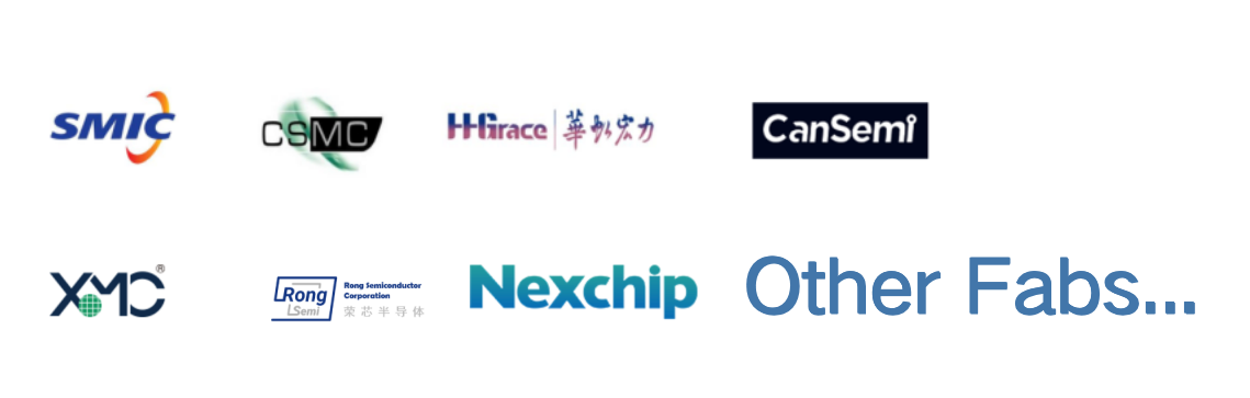
SMIC
A Comprehensive Fab which can provide turnkey service from design to test, tape out servie ranging from 0.35 um to 28 nm.
CSMC
Runs the largest 6-inch foundry line and an 8-inch foundry line in mainland China.
HH grace
Be known as an 8-inch wafer Fab and can make smallest chip size under equivalent specifications.
Nexchip
A emerging 12-inch wafer Fab in mainland China.
Cansemi
A 12-inch wafer Fab that meets customized demands, focusing on application fields such as the IOTs, Automotive Electronics, and 5G.
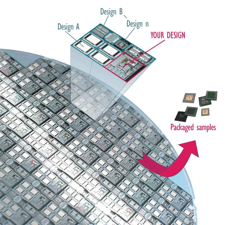
MPW
MPW (Muti Project Wafer) Service:Designs using the same process are fabricated on a single wafer. Each designer get small number of dies that are sufficient for experimentation and testing. The manufacturing cost is shared among all participating MPW projects based on the chip area, in which way can reduce both costs and new product development risks, thereby increase the new design efficiency. Waifu maintain close collaboration with major foundries worldwide as well as local foundries in China on MPW initiatives.
____________________________________________________________________________________________________________________________
Engineering Wafer Run
Producing complete photomasks and a small number of wafers (typically 12 or 25 pieces) to obtain a certain quantity of chips for small-scale product promotion. Some wafers can be hold at certain stages to facilitate in-depth analysis of chip performance. Once there is sufficient market demand, the process can proceed to the Production Lot phase.
Production Lot
The cost per wafer is significantly reduced and satisfy continue market demand.
Services WeProvide
Waifu can provide services in following aspects in the Foundry Services
◇Technology Nodes & Fabs Comparison and Selection Guidence
◇Provision of Foundry Files Needed for Design
◇Assistance with Tape-Out Process
◇Wafer Production WIP Reports Monitoring
◇Design Modifications and Information Management
◇Wafer Storage and Release, Quality Feedback and Control
◇Wafer Logistics and Delivery Services
◇Subsequent Packaging and Testing Services